ENGINEERING PCB ADVANTAGES

Four PCB capabilities engineers notice first.

This page focuses on the four capability areas that separate FQC from commodity PCB fabs. High layer count, process stability, fine-line density, and high-speed / high-frequency builds.

FQC specialty capability showcase
FOUR ENGINEERING ADVANTAGES

The specs that matter before quoting.

High-layer multilayer product - FQC
01

High-layer multilayer product - FQC

HIGH LAYER COUNT

50-layer multilayer builds, with an 80L / 100L roadmap

For engineers, layer count is not just a marketing number. It means the fab can keep registration, press-cycle stability, hole reliability, and impedance control under control as the stack grows.

FQC's disclosed product examples include 50-layer multilayer builds, while the Thailand technical table lists 80 layers for 2026 and 100 layers for 2027 planning. That gives buyers a credible path from demanding multilayer programs into future ultra-high-layer designs.

Best fit: AI server boards, ATE / test-interface boards, dense industrial control hardware, and high-pin-count systems where routing escape and power integrity push beyond standard multilayer capability.

Max layer count

50L proven; 80L / 100L roadmap

Aspect ratio

25:1 now; 30:1 target

Impedance tolerance

±7% now; ±5% target

Layer-to-layer registration

0.05 mm now; 0.035 mm target

Proof

PPT capability table: 80L in 2026 planning, 100L in 2027 planning; product examples include 50L multilayer cross sections.

Reliability inspection and process control - FQC
02

Reliability inspection and process control - FQC

PROCESS STABILITY

Reliability controls for boards that cannot fail in the field

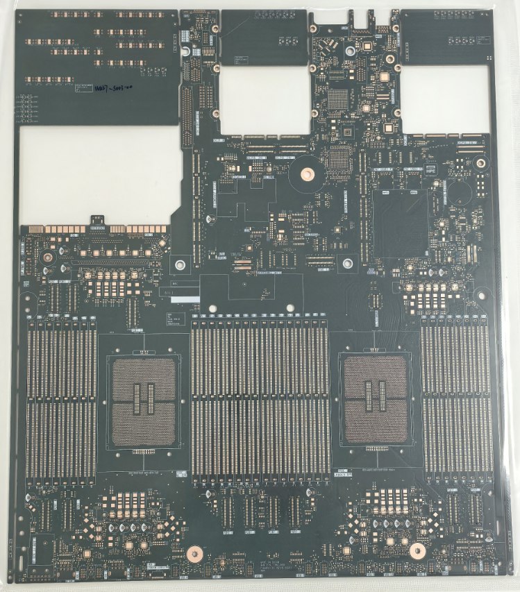
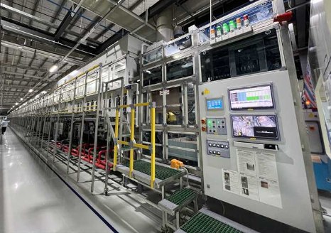
High-reliability PCB work is won in process control: material traceability, change-point discipline, coupon testing, cross-section analysis, and repeatable plating / lamination behavior from lot to lot.

The Thailand profile calls out IATF 16949, ISO 13485, QC080000, 4M1E change-point management, lot guarantee testing, shipment coupons, and long-term retained samples. That matters to engineers building automotive, medical, industrial, and instrumentation programs.

Best fit: long-life industrial electronics, automotive control boards, medical instrumentation, safety-related assemblies, and products where one lot excursion creates field-service cost.

Quality systems

IATF 16949 / ISO 13485 / QC080000

Change control

4M1E + 3H change-point management

Lot testing

Thermal shock + cross-section

Traceability

Shipment coupon + retained sample

Proof

Lot coupon testing includes thermal shock cycling and cross-section checks; retained samples support traceability programs.

Fine-line HDI product - FQC
03

Fine-line HDI product - FQC

HIGH-DENSITY ROUTING

35 um class fine line, microvia, and HDI capability

High density is where many standard fabs lose manufacturability. Fine traces, tight spacing, small laser vias, and repeated lamination cycles leave very little room for registration drift.

The PPT lists minimum inner / outer line and space at 0.035 / 0.035 mm for 2026, with a 0.025 / 0.025 mm 2027 target. It also lists HDI builds up to 4+N+4 in 2026 and 5+N+5 in 2027, with laser vias down to 0.075 mm and a 0.05 mm target.

Best fit: high-density BGA escape, optical modules, compact industrial controllers, AI accelerator carriers, and layouts where board area is constrained but I/O count keeps rising.

Line / space

35 / 35 um now; 25 / 25 um target

Min laser via

0.075 mm now; 0.05 mm target

Build-up order

4+N+4 now; 5+N+5 target

Pattern accuracy

±0.05 mm now; ±0.035 mm target

Density window

2026: 35 / 35 um L/S and 0.075 mm laser via; 2027 target: 25 / 25 um L/S and 0.05 mm laser via.

High-speed low-loss PCB - FQC
04

High-speed low-loss PCB - FQC

HIGH-SPEED / HIGH-FREQUENCY

40 GHz signal integrity with HDI stackups

High-speed boards need more than a low-loss material name on a quotation. The fab has to control impedance, copper roughness, dielectric thickness, registration, and via structures through the production flow.

FQC's materials and process base includes high-speed laminates such as Panasonic, Rogers, Isola, TUC, and related PCB material systems. The equipment list also includes network-analyzer capability, while existing case-study content references 40 GHz optical-module signal integrity.

Best fit: 800G / 1.6T optical modules, high-speed server interconnects, 5G / RF boards, automotive radar-related builds, and designs where insertion loss and impedance variation drive pass / fail.

Tolerance

±7% now; ±5% target

Max frequency

40 GHz class

Qualified materials

Panasonic / Rogers / Isola / TUC

Target application

800G / 1.6T optical, RF, server

Proof

40 GHz class signal-integrity positioning, ±7% impedance in 2026 planning and ±5% in 2027 planning.

SURFACE FINISH / IN-HOUSE PORTFOLIO

Eight finishes. Zero outsourcing. One facility.

Every surface finish processed in-house in our Rayong, Thailand facility. No subcontracting. No quality handoff. No lead-time slippage.

FQC Rayong surface finish line
Finishes8
In-house100%
Outsourcing0%
Apr 2026+1
FIN-01 · FIN-09

The surface-finish portfolio.

Each process — chemistry, spec window, applications, trade-offs. All run under one roof, one QMS.

FIN-01

LF HASL (Sn-Ni-Cu)

Tin-Nickel-Copper lead-free alloy

Thickness
2 – 40 μm
Process Temp
245 – 260°C
Shelf Life
12 mo
Cost Tier
▌▌░░░
Applications
  • Consumer electronics
  • Automotive general
  • Industrial
Pros
  • Economical
  • Repairable
  • Strong solderability
Cons
  • !Uneven surface
  • !Not for fine-pitch BGA
FIN-02

LF HASL (Sn-Ag-Cu)

Tin-Silver-Copper SAC alloy

Thickness
2 – 40 μm
Process Temp
235 – 245°C
Shelf Life
12 mo
Cost Tier
▌▌▌░░
Applications
  • Industrial
  • Telecom backplanes
Pros
  • Superior solder joint strength
  • Lead-free compliant
Cons
  • !Uneven surface limits fine-pitch
FIN-03

ENIG

Electroless Nickel Immersion Gold · Ni-P (4-7 μm) + Au (0.05-0.15 μm)

Thickness
Au 0.05-0.15 / Ni 3-8 μm
Process Temp
Ambient
Shelf Life
12 mo
Cost Tier
▌▌▌▌░
Applications
  • BGA/CSP fine-pitch
  • Medical
  • Aerospace
Pros
  • Flat surface
  • Excellent solderability
  • Wire-bondable
Cons
  • !Black-pad risk if over-processed
FIN-04

ENEPIG

Electroless Ni (3-6μm) + Pd (0.05-0.3μm) + Au (0.03-0.1μm)

Thickness
Total 3 – 6.4 μm
Process Temp
Ambient
Shelf Life
12 mo
Cost Tier
▌▌▌▌▌
Applications
  • High-reliability (aerospace, medical implants, MIL-SPEC)
Pros
  • Au/Al wire bondable
  • No black pad
  • Multi-assembly tolerant
Cons
  • !Highest cost
FIN-05

Electro Soft Gold

Pure gold plating (99.9%+)

Thickness
0.3 – 3 μm
Process Temp
Ambient
Shelf Life
Indefinite
Cost Tier
▌▌▌▌▌
Applications
  • Gold wire bonding
  • Contact fingers
  • RF connectors
Pros
  • Lowest contact resistance
  • Ultra-high reliability
Cons
  • !Soft surface
  • !Expensive
FIN-06

Electro Hard Gold (CoHG / NiHG)

Gold + Cobalt or Nickel hardener

Thickness
0.3 – 2.5 μm
Process Temp
Ambient
Shelf Life
Indefinite
Cost Tier
▌▌▌▌▌
Applications
  • Card-edge connectors
  • Keypad contacts
  • Test points
Pros
  • Wear resistant
  • High conductivity
Cons
  • !Specialized application only
FIN-07

Immersion Tin

Pure tin immersion deposit

Thickness
0.8 – 1.2 μm
Process Temp
Ambient
Shelf Life
6 mo
Cost Tier
▌▌░░░
Applications
  • Press-fit connectors
  • Backplanes
  • Automotive
Pros
  • Flat coplanar surface
  • Low cost
Cons
  • !Tin-whisker risk
  • !Short shelf life
FIN-08

OSP

Benzimidazole / Benzotriazole organic film

Thickness
0.2 – 0.5 μm
Process Temp
Ambient
Shelf Life
6 mo
Cost Tier
▌░░░░
Applications
  • High-volume consumer
  • Single-reflow boards
Pros
  • Cheapest
  • Flat
  • Naturally lead-free
Cons
  • !Handling-sensitive
  • !Not re-workable
COMING APR 2026
FIN-09

Immersion Silver

Pure silver immersion deposit

Thickness
0.1 – 0.4 μm
Process Temp
Ambient
Shelf Life
12 mo
Cost Tier
▌▌▌░░
Applications
  • RF / microwave
  • Automotive
  • Cost-optimized fine-pitch
Pros
  • RF performance > OSP
  • Flat
Cons
  • !Sulfide tarnishing if humid
Status

Capability installation April 2026 · Production qualification Q2 2026

PROCESS FLOW · REV A

Surface finish as one node in the full flow.

Bare-CCL through ship-out. Double-layer and multi-layer / HDI routes share the surface-finish bay — one line, all stackups.

CCL CuttingWarehouseLay upLaminationHeat StakeMech / Laser DrillCu PlatingB/OInner AOIInner PatternOuter PatternOuter AOIDrill SharpeningResin PluggingFlying ProbeSM PretreatSM PrintSymbolSurface FinishSURFACE FINISHV-CutCleaningImm Tin / OSPE-Test / FQCWarehouseShipping
Double layer
Multi-layer & HDI
Surface Finish
WHY IN-HOUSE MATTERS

Four things subcontracting loses.

The cost of owning the finishing lines vs. routing panels to a vendor-of-vendor.

01Lead time

No transit between subcontractors. Direct process handoff saves 3–5 days per order.

02Quality control

Every finish qualified under our own IATF 16949 QMS — no external QC-basis gap.

03Flexibility

Switch finish type mid-order. Adjust thickness spec on short notice.

04Traceability

Single-facility lot genealogy from bare CCL through final finish.

NEXT STEP

Not sure if your project fits.

Talk to an engineer, or send Gerbers for a DFM review.

Request a DFM review